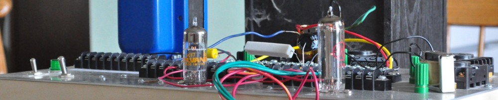
So I was looking over the prototype work I’d done for a 6336 Dual Triode SET amp driver stage. This is the unit that I discussed on the “Brassboard Prototypes” page. However, when examining the pictures and performance, I noticed that something wasn’t quite right. So I took apart the brassboard and took a look. Sure enough, I had built the unit slightly differently than what was in the written schematic on that page.
One change is that I replaced the 470kΩ resistors listed on the schematic with 499kΩ resistors in the brassboard. These are grid leak resistors and in these positions, the 6% increase probably won’t have a major impact on overall performance. The bigger issue was that instead of using the 0.068µf coupling capacitors listed on the schematic, I had instead used 0.047µf capacitors in those positions. Now wth two cascaded stages, this could have an impact on the calculated low end rolloff. The other thing I did was instead of bypassing the first stage cathode resistor with a 10µf capacitor I used a 22µf instead. This may have partially offset the effects of the coupling capacitors, so that I did’t notice in initial testing. Clearly I need to revisit my data.
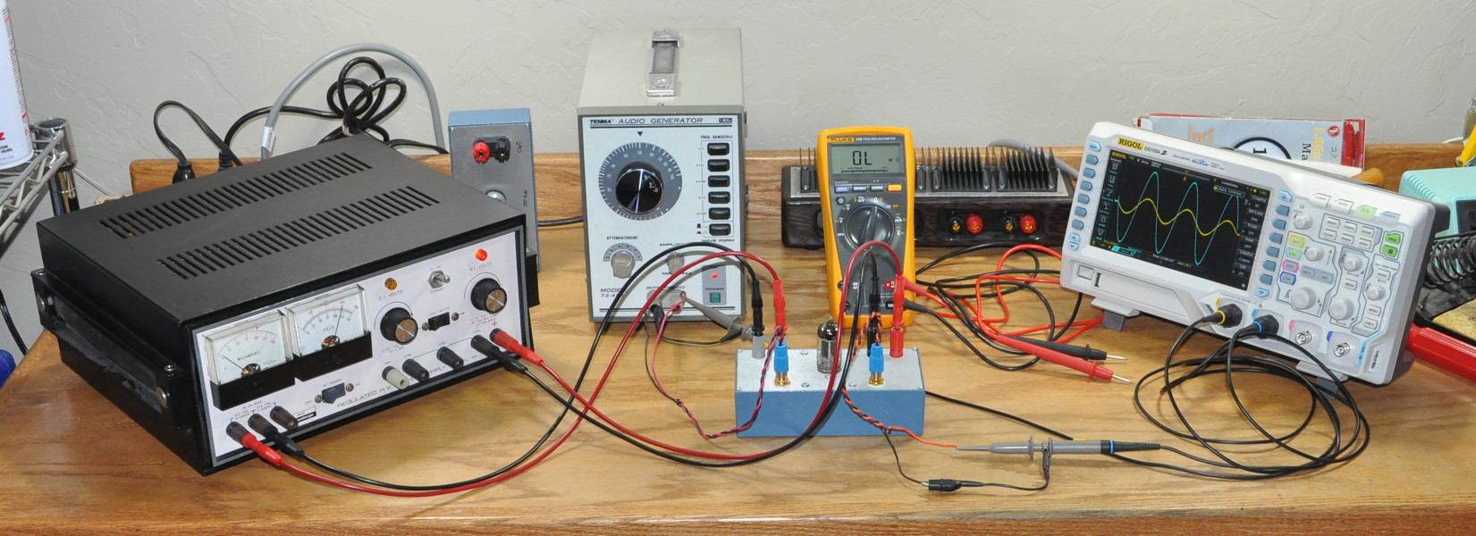
In addition to these discoveries, something else has changed on my bench. When I first put this brassboard together, for testing I used my tried and true B+K 1477 dual trace analog oscilloscope. Now this was a fine scope in it’s day but it is a little rough for precision work. Since then, I have upgraded to a modern Rigol 1054Z four channel scope which is much more capable. As such, I decided that I would redo the testing of the brassboard driver in its “as built” configuration. Here’s the test setup:
First off, just for reference, here is the schematic showing how the brassboard was actually put together. This schematic shows the actual component values used in the unit.
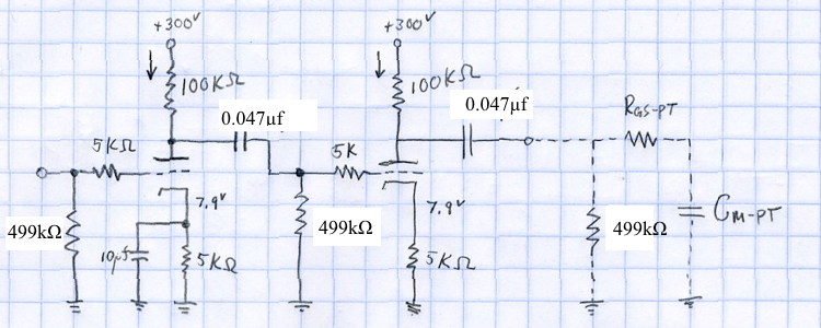
Please note that whereas the final 499kΩ resistor is included in the unit, the terminating grid-stopper resistor and Miller capacitance are not.
So the first thing I did was rerun the bandwidth check. I ran frequencies from 10Hz to 100000Hz so I could clearly see the bandpass characteristic of the driver. Also note that I ran this at an input voltage of 1v RMS. This produces an output swing of over 77v RMS (or almost+/- 110v peak). I did this because I wanted the bandpass data to reflect the worst case performance given the very large voltage swings. At lower drive levels the data should just get cleaner. Here is the data table:
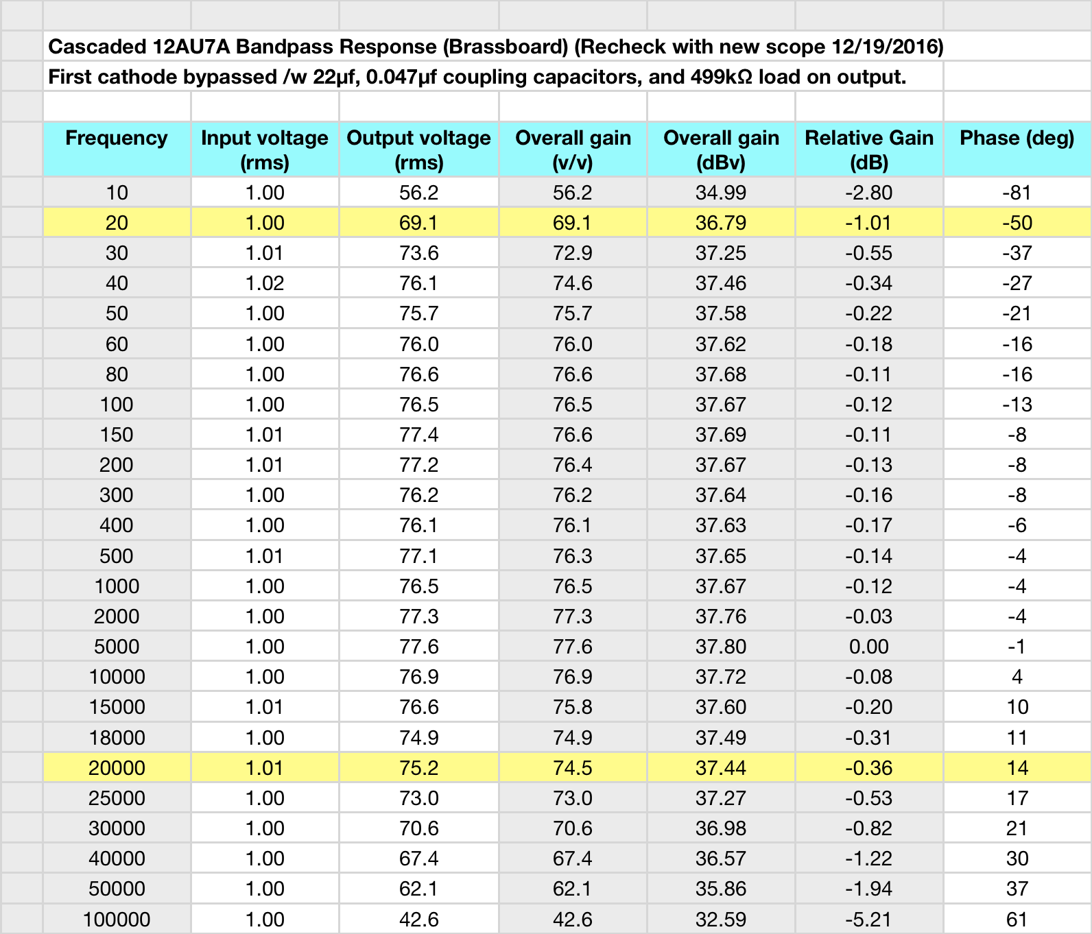
I measured the input voltage, output voltage, and phase shift at each frequency. I will use these same frequencies when I test the entire 6336 SET amp after completion. I have highlighted the 20Hz and 20kHz limits for reference. Here are the gain plots generated from this data:
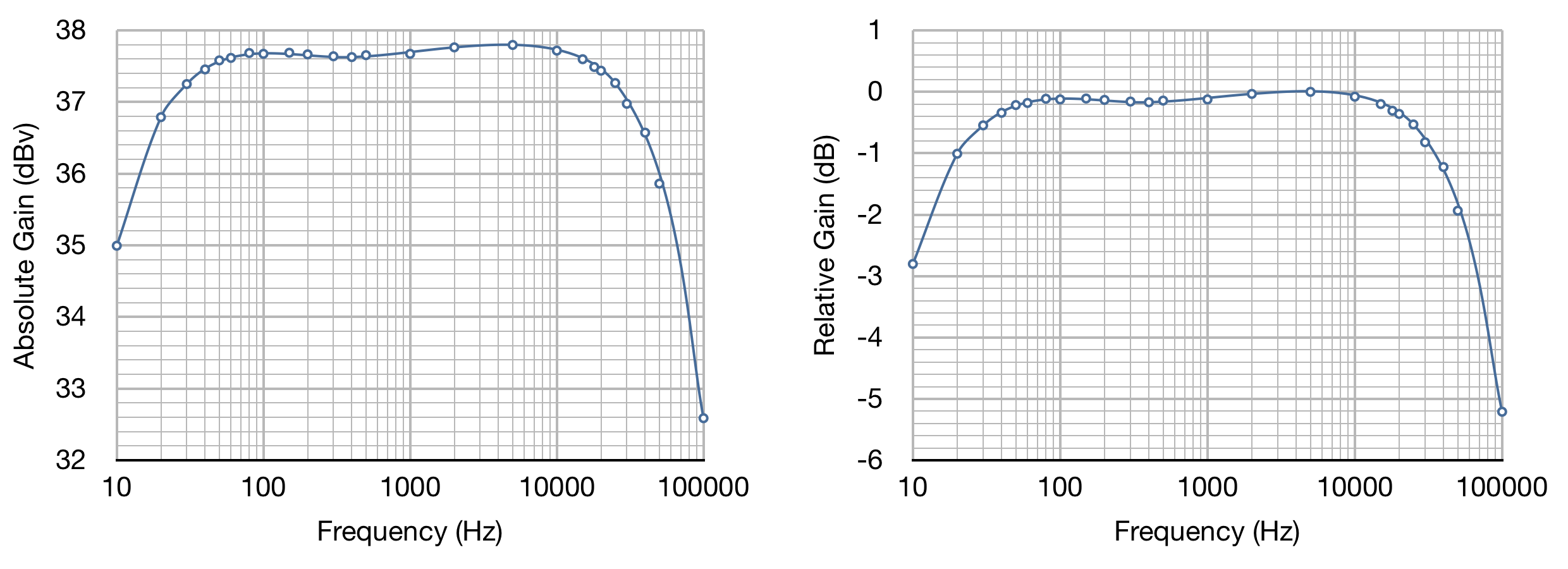
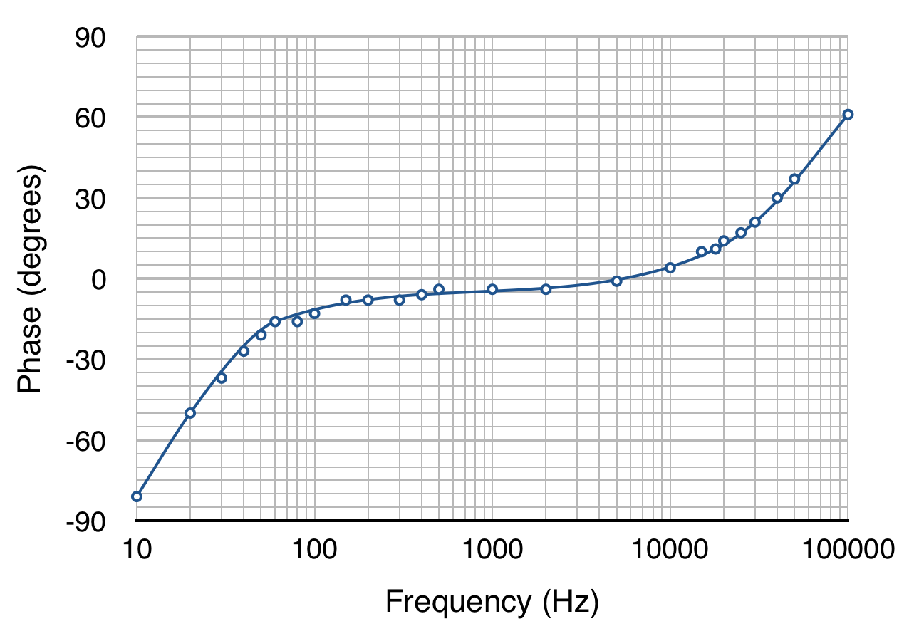
The driver has a flat and well behaved passband with gentle rolloff at both ends. And, as we would expect from a pass band like this, the phase response is also very well behaved. Here is what it looks like:
The other thing I did was to check the nominal gain and distortion numbers. I did this at three different output voltage levels. One at an output voltage of +/-82v peak, one at a slightly lower value of about +/-75v peak, and one at a much lower output level of about +/-11v peak. The first level is because the target amplifier has a power stage biased at 81v. This tells me what the driver distortion looks like just as the power stage enters the overdrive condition. The second condition is about one dB down from the overdrive condition and represents the reference maximum drive condition for the amplifier. The third number is 17.4dB down from the overdrive condition and represents a good midrange approximation of the distortion under most listening conditions.
The table below contains the gain data, the distortion levels for 2nd, 3rd, and 4th harmonics, and the total harmonic distortion (THD) at each drive level. All three conditions were measured at 5kHz (which is the nominal peak gain point for the driver stage).
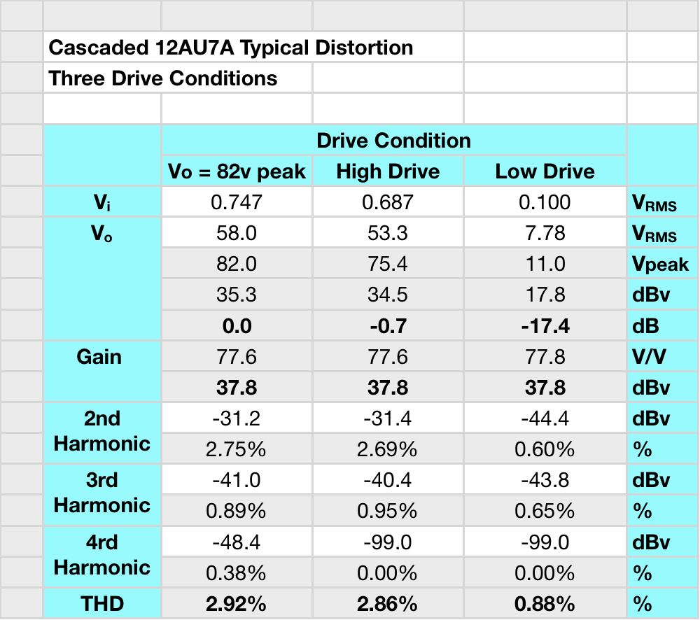
This data represents reasonable distortion performance for a cascaded driver of this type. I am happy with these results and think I’ll be building the final amplifier with these circuit values rather than the ones in the original schematic. The smaller coupling caps result in much lower bias excursion recovery times. And the larger cathode bypass capacitor on the first stage doesn’t bother me because, with the stage biased to almost 8v, the probability of a cathode driven bias excursion on this stage is very virtually impossible under any conceivable operating condition.
I’m glad that I noticed this and decided to take a look. Just another reminder that sometimes it really pays off to check our work.
Thoughts?
Pingback: One Last SET Driver Check | Cascade Tubes
Pingback: Design Decisions | Cascade Tubes
Glad to see your blog hiatus is over. Now I get to enjoy catching up.
The text consistently mentions the 22 mFd bypass on the first cathode but the schematic still reflects 10. Did I miss something?
Also, can you comment on the use of the cathode bypass on the first, rather than the second stage? (or both or neither) It looks like both stages here are (nearly) zero current voltage amplifiers. I’m used to seeing cathode bypassing later in the circuit and thought its main purpose was to provide additional “AC stiffness” to the cathode as voltage and current swings become larger.
Jim;
As to the cathode bypass, you are entirely correct. I did use a 22µf but I did not correct the schematic. A mistake on my part for which I apologize profusely.
The reason for bypassing the first cathode rather than the second has to do with distortion. The first stage has far lower plate voltage swing than the second. Because, in triode stages, distortion is mostly 2nd harmonic and proportional to output swing, then it make sense (if you need the additional gain afforded by using cathode bypass) to bypass the first stage where swing in lowest. Then cathode degeneration of the second stage then helps control overall distortion in its much larger output swing.
Not bypassing the cathode has two affects. The first is that it reduces stage gain due to cathode degeneration (this is single stage, i.e. local, negative feedback). The second is the reduction of overall distortion due to that negative feedback. I’m not quite sure what you mean by “AC stiffness” as, in a well designed stage, cathode bypass has virtually no effect on transient response.