The “Color” preamp has been checked out on the test bench and everything is working per design. Bias points are good and the gain stage is operating exactly as designed. However, the buffer design I used was from a different project, and it operates differently in this project than the last one.
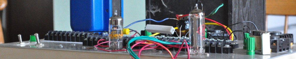
This may seem nonintuitive, and it was to me until I reread my design notebook section on cathode follower design. After reading what I had written, I rechecked some calculations and I am convinced it is working properly and per the design. Here is the unit under test on my workbench.

In operation the grid circuit of the buffer stage was being overloaded at a significantly lower voltage than at what I thought it should. This led to a full day of design investigations until I convinced myself that I understood exactly how the circuit was functioning.
This led me to make a slight change to the circuit to ensure good performance over a range of conditions. But it also means that instead of having a gain range of approximately -20dB to +20dB the gain range is more like -26dB to +14dB. I don’t really see this as an issue as most solid state amps are very sensitive and too much signal is often more of a problem than too little signal.
I still have some significant testing to perform. When that’s completed I’ll make a longer post with all the salient information.
As always, questions and comments are welcome.